- 您现在的位置:买卖IC网 > Sheet目录3884 > PIC16F628T-04E/SO (Microchip Technology)IC MCU FLASH 2KX14 18-SOIC
2009 Microchip Technology Inc.
DS40044G-page 143
PIC16F627A/628A/648A
17.5
Timing Parameter Symbology
The timing parameter symbols have been created with one of the following formats:
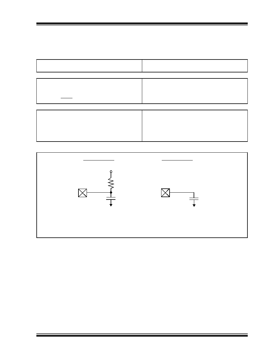
FIGURE 17-3:
LOAD CONDITIONS
1. TppS2ppS
2. TppS
T
F
Frequency
T
Time
Lowercase subscripts (pp) and their meanings:
pp
ck
CLKOUT
osc
OSC1
io
I/O port
t0
T0CKI
mc
MCLR
Uppercase letters and their meanings:
S
FFall
P
Period
HHigh
R
Rise
I
Invalid (High-impedance)
V
Valid
L
Low
Z
High-Impedance
VDD/2
CL
RL
Pin
VSS
CL
RL =464
Ω
CL = 50 pF for all pins except OSC2
15 pF for OSC2 output
Load Condition 1
Load Condition 2
发布紧急采购,3分钟左右您将得到回复。
相关PDF资料
PIC18F448T-I/L
IC MCU FLASH 8KX16 W/CAN 44-PLCC
PIC18LF448T-I/L
IC MCU FLASH 8KX16 LV CAN 44PLCC
PIC18LF458T-I/L
IC MCU FLSH 16KX16 LV CAN 44PLCC
PIC16F627-04E/P
IC MCU FLASH 1KX14 18-DIP
PIC16F627-20E/P
IC MCU FLASH 1KX14 18-DIP
PIC16C54C-20I/P
IC MCU OTP 512X12 18DIP
PIC16F627T-04E/SO
IC MCU FLASH 1KX14 18-SOIC
PIC18LF448-I/L
IC PIC MCU FLASH 8KX16 44PLCC
相关代理商/技术参数
PIC16F628T-04E/SS
功能描述:8位微控制器 -MCU 3.5KB 224 RAM 16 I/O RoHS:否 制造商:Silicon Labs 核心:8051 处理器系列:C8051F39x 数据总线宽度:8 bit 最大时钟频率:50 MHz 程序存储器大小:16 KB 数据 RAM 大小:1 KB 片上 ADC:Yes 工作电源电压:1.8 V to 3.6 V 工作温度范围:- 40 C to + 105 C 封装 / 箱体:QFN-20 安装风格:SMD/SMT
PIC16F628T-04I/SO
功能描述:8位微控制器 -MCU 3.5KB 224 RAM 16 I/O RoHS:否 制造商:Silicon Labs 核心:8051 处理器系列:C8051F39x 数据总线宽度:8 bit 最大时钟频率:50 MHz 程序存储器大小:16 KB 数据 RAM 大小:1 KB 片上 ADC:Yes 工作电源电压:1.8 V to 3.6 V 工作温度范围:- 40 C to + 105 C 封装 / 箱体:QFN-20 安装风格:SMD/SMT
PIC16F628T-04I/SS
功能描述:8位微控制器 -MCU 3.5KB 224 RAM 16 I/O RoHS:否 制造商:Silicon Labs 核心:8051 处理器系列:C8051F39x 数据总线宽度:8 bit 最大时钟频率:50 MHz 程序存储器大小:16 KB 数据 RAM 大小:1 KB 片上 ADC:Yes 工作电源电压:1.8 V to 3.6 V 工作温度范围:- 40 C to + 105 C 封装 / 箱体:QFN-20 安装风格:SMD/SMT
PIC16F628T-20/SO
功能描述:8位微控制器 -MCU 3.5KB 224 RAM 16 I/O RoHS:否 制造商:Silicon Labs 核心:8051 处理器系列:C8051F39x 数据总线宽度:8 bit 最大时钟频率:50 MHz 程序存储器大小:16 KB 数据 RAM 大小:1 KB 片上 ADC:Yes 工作电源电压:1.8 V to 3.6 V 工作温度范围:- 40 C to + 105 C 封装 / 箱体:QFN-20 安装风格:SMD/SMT
PIC16F628T-20/SS
功能描述:8位微控制器 -MCU 3.5KB 224 RAM 16 I/O RoHS:否 制造商:Silicon Labs 核心:8051 处理器系列:C8051F39x 数据总线宽度:8 bit 最大时钟频率:50 MHz 程序存储器大小:16 KB 数据 RAM 大小:1 KB 片上 ADC:Yes 工作电源电压:1.8 V to 3.6 V 工作温度范围:- 40 C to + 105 C 封装 / 箱体:QFN-20 安装风格:SMD/SMT
PIC16F628T-20E/SO
功能描述:8位微控制器 -MCU 3.5KB 224 RAM 16 I/O RoHS:否 制造商:Silicon Labs 核心:8051 处理器系列:C8051F39x 数据总线宽度:8 bit 最大时钟频率:50 MHz 程序存储器大小:16 KB 数据 RAM 大小:1 KB 片上 ADC:Yes 工作电源电压:1.8 V to 3.6 V 工作温度范围:- 40 C to + 105 C 封装 / 箱体:QFN-20 安装风格:SMD/SMT
PIC16F628T-20E/SS
功能描述:8位微控制器 -MCU 3.5KB 224 RAM 16 I/O RoHS:否 制造商:Silicon Labs 核心:8051 处理器系列:C8051F39x 数据总线宽度:8 bit 最大时钟频率:50 MHz 程序存储器大小:16 KB 数据 RAM 大小:1 KB 片上 ADC:Yes 工作电源电压:1.8 V to 3.6 V 工作温度范围:- 40 C to + 105 C 封装 / 箱体:QFN-20 安装风格:SMD/SMT
PIC16F628T-20I/SO
功能描述:8位微控制器 -MCU 3.5KB 224 RAM 16 I/O RoHS:否 制造商:Silicon Labs 核心:8051 处理器系列:C8051F39x 数据总线宽度:8 bit 最大时钟频率:50 MHz 程序存储器大小:16 KB 数据 RAM 大小:1 KB 片上 ADC:Yes 工作电源电压:1.8 V to 3.6 V 工作温度范围:- 40 C to + 105 C 封装 / 箱体:QFN-20 安装风格:SMD/SMT